User Rambo5 uploaded the image
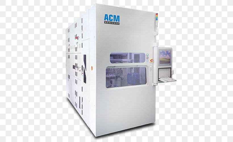
The image shows a white-colored industrial machine with the letters "ACM" on the top left corner. The machine appears to be a control panel with multiple buttons and switches on the left side. On the right side, there is a large window with a view of a blue-colored machine inside. The window is open, allowing natural light to enter the machine. There is also a small screen on the front of the machine, which is likely displaying information about the machine's functions. This machine is likely used for manufacturing or testing purposes.
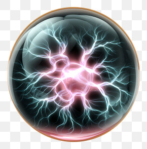
Plasma Etching Semiconductor Wafer Glass Etching PNG
. The resolution of this PNG file is 500 x 500 pixels and it has a file size of 226.60 KB.The image shows a white-colored industrial machine with the letters "ACM" on the top left corner. The machine appears to be a control panel with multiple buttons and switches on the left side. On the right side, there is a large window with a view of a blue-colored machine inside. The window is open, allowing natural light to enter the machine. There is also a small screen on the front of the machine, which is likely displaying information about the machine's functions. This machine is likely used for manufacturing or testing purposes.
Related PNG Images