Save
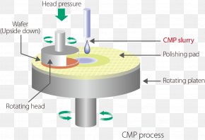
User myenemy uploaded this Technology - Chemical-mechanical Planarization Front End Of Line Back End Of Line Semiconductor High-κ Dielectric PNG PNG image on December 27, 2017, 7:00 am. The resolution of this file is 1443x806px and its file size is: 441.26 KB. This PNG image is filed under the tags:
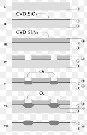
Technology - Chemical-mechanical Planarization Front End Of Line Back End Of Line Semiconductor High-κ Dielectric PNG
Below are more related PNG images...